Primary tabs

Contacts
e-mail: alessandro.molle@cnr.it
Skype ID: alessandro_molle
X: @AlessandroMolle
Website: https://alessandromolle.wixsite.com/xfab
ORCID ID: 0000-0002-3860-4120
ResearcherID: D-8952-2013
Scopus Author ID: 15123116600
News
 Alessandro will be co-organizing the Symposium B at the
in Strasbourg, France, 26-30 May 2025
Alessandro Molle is among the meeting chairs of the MRS 2024 Fall Meeting


Alessandro on the World's Top 2% Scientist List in the year:
2020, 2021, 2022, 2023, 2024
released by the Elsevier and Stanford University.

Alessandro Molle recognised
as 2022 RSC Outstanding Reviewers
for journal Nanoscale and Nanoscale Horizons.

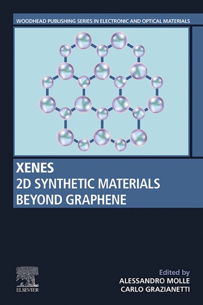 The Book of the Xenes
by Alessandro Molle & Carlo Grazianetti (Eds.)
(July 1st, 2022)
This is the first full-comprehensive book of the Xenes. You can find the updated list of nowadays available Xenes, and all their relevant properties and applications.
Available for purchase at the Elsevier website.
Job Openings
- 2D and topological materials for THz applications
- Molecular beam epitaxy of Xene layers and heterostructures;
- Chemical vapor deposition of transition metal dichalcogenides for nanoelectronics;
- Chemical vapor deposition of 2D materials for THz and far-IR applications;
- Processing and nanofabrication of electronic and optoelectronic devices based on 2D materials;
- Opto-thermo-electrical, chemical and structural characterization of 2D materials.

PI of:
ERC CoG 2017 "XFab" Grant N. 772261
ERC PoC 2022 "XMem" Grant N. 101069262
ERC PoC 2023 "TNext" Grant N. 101187967
Press release, @StampaCnr
https://www.cnr.it/it/intervento-presidente/7799/assegnato-al-cnr-un-consolidator-grant-dell-erc
Xenes on the media
TV & Radio & Social Media
CNR-IMM YT channel: Il Silicene e nuovi materiali: una rivoluzione per la nanotecnologia? (IT speaking)
RaiPlay - Superquark+ (Sept. 2020) [ita]
Rai 3 - TGLeonardo (2019) [ita]
RaiPlay - Rai Cultura (2019) [ita]
E-MRS Tv (2019) [eng]
Rai1-UnoMattina (11 Dec 2017) [ita]
Rad io3 [ita]
Radio24 "SmartCity" (8 March 2017)
Newspapers
Il Sole24Ore "Scenari" (2 March 2020)
La Stampa "TuttoScienze" (2018)
Il Sole24Ore "Nova" (3 Dec 2017)
About
Short Bio. Alessandro Molle graduated in 2001 at the University of Genova (Italy) with a master thesis on the nanocrystal formation during the homoepitaxial growth Al/Al(110). He obtained the PhD degree in Materials Science at the same University in April, 2005 with a thesis on metal nanostructure. In February 2005, he joined the MDM National Laboratory (formerly with INFM, now with the CNR-IMM) as a Post-Doc Fellow involved in the Molecular Beam Epitaxial Growth of high-k oxide thin films on semiconductor and of semiconductor thin films on metal oxides within the European Project ET4US. He was then involved in the surface passivation of high-mobility semiconductors (Ge and III-V compunds), for the subsequent deposition of high-k materials targeting ultra-scaled metal oxide semiconductor (MOS) structures for a Post-Si era of digital devices (in the framework of bilateral collaboration projects with IMEC, Belgium).
He was the principal investigator at CNR-IMM in the research activity related to the European Project "2D-Nanolattices: Strongly Anisotropic Graphite-like Semiconductor-Dielectric 2D Nanolattices" started from June 1st, 2011.The core-idea of that activity is to identify the basic properties of the epitaxial silicene, namely the silicon counterpart of graphene, including the structural arrangement, the elelctronic state, and the vibrational spectrum. Integration of epitaxial silicene in a field effect transistor has been achieved in collaboration with the group of Prof. Akinwande, Univ. of Texas at Austin. He currently supervised the unit activity on 2D materials beyond graphene including the epitaxial growth of Xenes (silicene, germanene, stanene, and phosphorene) on substrates, and the chemical vapor deposition of flat and patterned nanosheets of transistion metal dichalcogenides (MoS2, WS2, etc.). He has been awarded an ERC-COG 2017 grant (XFab) on the fabrication and technological implementation of Xenes and an ERC-PoC 2022 grant (XMem).
Skills. Molecular Beam Epitaxy (MBE) and in situ surface characterization (RHEED, XPS, LEIS, STM);
Admittance spectroscopy and electrical characterization of MOS capacitor;
Raman scattering spectroscopy.
Projects. Local PI in the framework of the the FP7 FET-Open project "2D-Nanolattices" (201-14); PI of the CNR grant "Joint Lab" in collaboration with the group of Prof. Akinwande, Univ. of Texas at Austin (2014-17); PI of the "CrystEL" project founded by the Fondazione CARIPLO and Regione Lombardia aiming at the enhanced competitiveness within the ERC calls (18 month since Oct. 2016), and local PI of the regional project "I-ZEB" founded by Regione Lombardia and CNR; Local PI of the I-ZEB project funded by Regione Lombardia; PI of the ERC-COG 2017 grant "XFab" and ERC-PoC 2022 grant "XMem".
Dissemination. In 2010, he co-chaired Symposium H "Post-Si CMOS electronic devices: the role of Ge and III-V materials" at the E-MRS 2010 Spring Meeting; Symposium I "The route to Post-Si CMOS devices: from high-mobility channels to graphene-like nanosheets" at the E-MRS 2013 Spring Meeting, Strasbourg, the Symposium Z "Two-dimensional crystals and their van der Waals heterostructures for nanoelectronics", E-MRS 2016 Spring Meeting, Lille; Symposium NM06 "Theory and Characterization of 2D Materials - Bridging Atomic Structutre and Device Performance", MRS 2020 Spring Meeting, Phoenix (AZ).
He is co-editor of the book "2D materials for nanoelectronics" published CRC Press (Taylor & Francis group), April 2026, and co-editor of the book "Xenes", published by Elsevier, Woodhead Publishing, July 2022. He is co-authors of two topical reviews ("Silicene:A review of recent experimental and theoretical investigations" published by J. Phys: Cond. Matter and "Two-dimensional silicon: the advent of silicene" published on 2D Materials) and a monographic chapter on the topic of silicene and Xenes. He is author and co-athor of more than 75 peer-reviewed articles in international scientific journals, he received more than 20 invitations to international conferences (including APS, ECS , and AVS meeting) for his contributions to the Ge/III-V issues and 2D materials issues, and he served as reviewer for European universities and institutions, and for several scientific journals (including Advanced Materials, Nano Letters, Physical Review Letters,).
Find me on:
Editorials
Highlights
2022
Optothermal silicene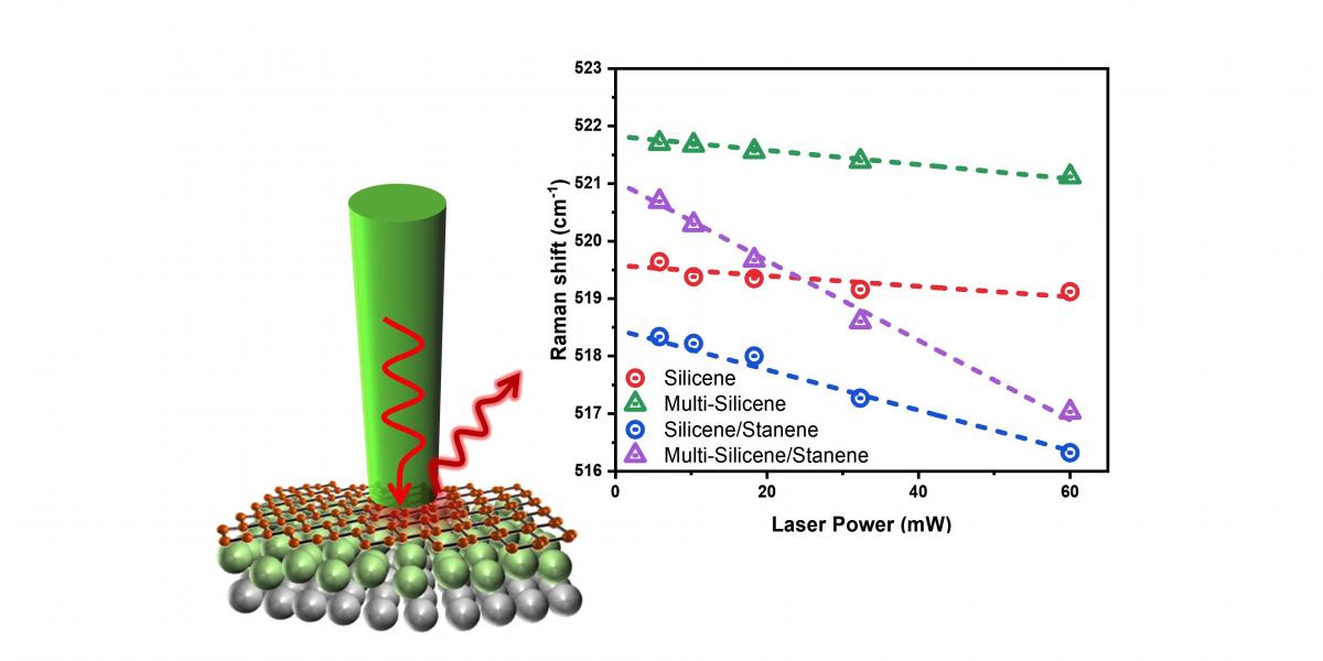
Eleonora Bonaventura*, Daya Sagar Dhungana, Christian Martella*, Carlo Grazianetti*, Salavtore Macis, Stefano Lupi, Emiliano Bonera, Alessandro Molle,* "Optical and thermal responses of silicene in Xene heterostructures" Nanoscale Horiz. 2022 (open access) https://doi.org/10.1039/D2NH00219A
2021
Two-dimensional Xene heterostructures
Daya Sagar Dhungana, Carlo Grazianetti*, Christian Martella, Simona Achilli, Guido Fratesi*, Alessandro Molle,* "Two-dimensional silicene-stanene heterostructures by epitaxy" Adv. Funct. Mater. 2021 https://doi.org/10.1002/adfm.202102797 (Open Access)
Can stanene grow on sapphire?
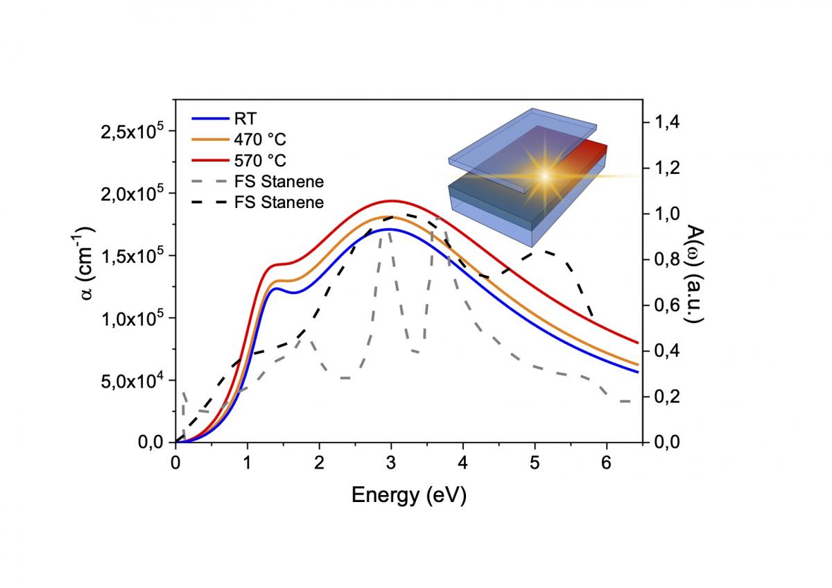
Carlo Grazianetti, Eleonora Bonaventura, Christian Martella, Alessandro Molle,* and Stefano Lupi*, "Optical Properties of Stanene-like Nanosheets on Al2O3(0001): Implications for Xene Photonics" ACS Appl. Nano Mater. 2021 https://dx.doi.org/10.1021/acsanm.0c03221 (Open Access)
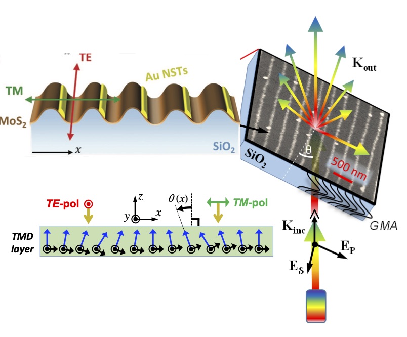
The MoS2 plasmonics quartet
M. Bhatnagar et al., "Broadband and Tunable Light Harvesting in Nanorippled MoS2 Ultrathin Films" ACS Appl. Mater. Interf. 2021 (Open Access);
A. Camellini et al., "Evidence of Plasmon Enhanced Charge Transfer in Large-Area Hybrid Au–MoS2 Metasurface" Adv. Opt. Mater 2020
C. Mennucci et al, "Geometrical Engineering of Giant Optical Dichroism in Rippled MoS2 Nanosheets" Adv. Opt. Mater. 2020
M. Bhatnagar et al.,"Ultra-broadband photon harvesting in large-area few-layer MoS2 nanostripe gratings" Nanoscale 2020 (Open Access)
2020
Epitaxial Phosphorene at hand
C. Martella, G. Faraone, M. H. Alam, D. Tanneja, L. Tao. G. Scavia, E. Bonera, C. Grazianetti, D. Akinwande, and A. Molle, "Disassembling Silicene from Native Substrate and Transferring onto an Arbitrary Target Substrate" Adv. Funct. Mater. 2020 https://doi.org/10.1002/adfm.202004546 (Open Access)
 2019
2019
Epitaxial Phosphorene at hand
C. Grazianetti, G. Faraone, C.Martella, E. Bonera, and A. Molle, "Embedding epitaxial (blue) phosphorene in between device-compatible functional layers" Nanoscale (2019) DOI: 10.1039/C9NR06037E (Open Acces)
2018
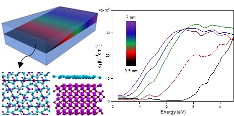
Optical conductivity of 2D silicon
C. Grazianetti, S. La Rosa, C. Martella, P. Targa, D. Codegoni, P. gori, O. Pulci, A. Molle*, and S. Lupi*, "Optical Conductivity of Two-Dimensional Silicon: Evidence of Dirac Electrodynamics" Nano Letters 2018, DOI: 10.1021/acs.nanolett.8b03169
All about silicene
A. Molle, C. Grazianetti*, L. Tao*, D. Taneja, Md. Hasibul Halam, and D. Akiwande*, "Silicene, silicene derivatives, and theri device applications" Chem. Soc. Rev. 2018, 47, 6370-6387 DOI:10.1039/C8CS00338F (2018)
Anisotropy at the 2D level by design
C. Martella, C. Mennucci, A. Lamperti, E. Cappelluti,
F. Buatier de Mongeot, and A. Molle*, "Designer Shape Anisotropy on 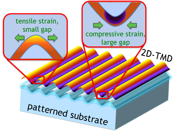 Transition-Metal-Dichalcogenide Nanosheets", Advanced Materials (2018), DOI: 10.1002/adma.201705615
2017
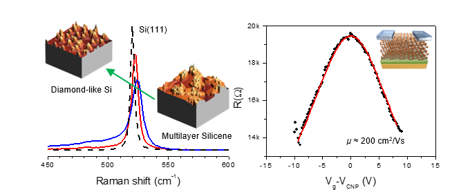
Silicene goes Multilayer!
C. Grazianetti, E. Cinquanta, L. Tao, P. De Padova, C. Quaresima, C. Ottaviani, D. Akinwande, and A. Molle, "Silicon Nanosheets: Crossover between Multilayer Silicene and Diamond-like Growth Regime" ACS Nano (2017), DOI: 10.1021/acsnano.7b00762
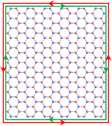
A perspective on two-dimensional Xenes
A. Molle, J. Goldberger, M. Houssa, Y. Xu, S.-C. Zhang, and D. Akinwande,
"Buckled two-dimensional Xene sheets",
Nature Materials, 16, 163 (2017) DOI: 10.1038/NMAT4802 (2017)
2015
The silicene transistor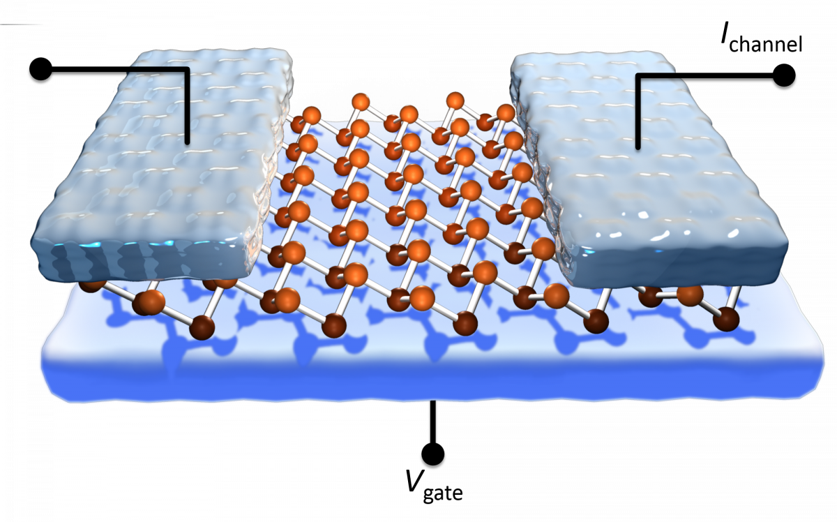
L. Tao, E. Cinquanta, D. Chiappe, C. Grazianetti, M. Fanciulli, M. Dubey, A. Molle, and D. Akinwande, "Silicene field-effect-transistors operating at room temperature" Nature Nanotechnology 10, 227 (2015), doi:10.1038/nnano.2014.325
See also: "2D Materials: Silicene Transistors", G. Le Lay, Nature Nnotechnology | News & Views, doi:10.1038/nnano.2015.10
Research
- 2D buckled Xene sheets. Growing new 2D materials of single element X ranging from silicene to germanene to stanene and phosphorene, generally termed Xenes, is a new research frontier aiming to expand the common knowledge in materials science, nanotechnology, and physics. The activity basically relies on the epitaxy on substrates and subsequent processing towards device integration. One approach is the encapsulation + delamination from cleavable substrates, see the realization of the silicene transistor here. An alternative aproach is Xene template engineering, namely the quest for substrate suitable for the commensurate growth or the van der Waals epitaxy of a Xene single layer. See the case of silicene on MoS2 here and the related heterosheet transistor here. MSc/PhD thesis openings available for this activity.
- Chemical vapor deposition of transistion metal dichalcogenides (TMDs) and their van der Waals heterostructures. TMDs like MoS2 are one of the more feasible 2D platform for nanotechnology. They can be utilized in nanoelectronics (eithr for logic and memory devices as well as for flexible electronics), optolectronics, photonics, chemical and bio- sensing, energy and hydrogen evolution reaction, etc. The big challenge for the TMD production is the large-scale synthesis. We address this issue by a cost-effective furnace-based chemical vapor deposition approach starting from a solid film precursor of the transition metal on a substrate (for more details see here). This approach enables us to have large area, conformal and thickness controlled TMD nanosheets that can be used as building blocks for van der Waal heterostructures. Target applications are: ultra-scaled field effect transistors, hybrid heterostructures for light emitting diodes and photovoltaic cells. MSc/PhD thesis openings available for this activity.
- Anisotropy at the 2D level. TMD as well graphene are isotropic in nature. Making them anisotropic may open a wealth of unexplored properties descending from the local manipulation of the 2D lattice. We induce a one-directional anisotropy in MoS2 nanosheet as a consequence of a conformal growth on a pre-patterned substrate. Target applications are: exciton engineering and strain tuning towards single photon emitter production, platforms for hydrogen evolution reaction. MSc thesis openings available for this activity.
- Transition metal ditellurides as Weyl semimetal ultrathin films. MoTe2 and WTe2 can be synthesized as ultrathin films and reduced to a octahedral phase hosting so-called Weyl fermions in their electronic structure. This may lead to to the emergence of topological Weyl semimetallic state in an ultrathin film configuration with high potential for technology applications. One example in this respect is the coupling with a ferromagnetic counterpart so as to follow new paths for spin manipulation towards spintronics forefronts. This route will be followed within the framework of a H2020 FET-Proactive project "Skytop" at the CNR-IMM.
Scientific Production
Materials Science in Semiconductor Processing [Pergamon], Volume: 188 Pages: 109247
Small [], Volume: 21 Issue: 7 Pages: 2406088
Wafer‐Scale Synthesis of Topological Insulator Sb2Te3 Thin Films
Advanced Materials Interfaces [], Pages: 2400961
Advanced Science [], Volume: 12 Issue: 1 Pages: 2570006
Advanced Optical Materials [], Volume: 12 Issue: 33 Pages: 2470107
The future of Xenes beyond graphene: challenges and perspective
2D Materials [IOP Publishing], Volume: 11 Issue: 4 Pages: 042005
Terahertz and Infrared Plasmon Polaritons in PtTe2 Type‐II Dirac Topological Semimetal
Advanced Materials [], Pages: 2400554
Advanced Science [], Pages: 2406703
Effects of inorganic seed promoters on MoS2 few-layers grown via chemical vapor deposition
Journal of Crystal Growth [North-Holland], Volume: 627 Pages: 127530
Large Area Growth of Silver and Gold Telluride Ultrathin Films via Chemical Vapor Tellurization
Inorganics [MDPI], Volume: 12 Issue: 1 Pages: 33
Effective Out‐Of‐Plane Thermal Conductivity of Silicene by Optothermal Raman Spectroscopy
Advanced Optical Materials [], Pages: 2401466
Silicene Applications in Nanotechnology: From Transistors to Bendable Membranes
Authorea Preprints [Authorea],
Advanced Materials [], Volume: 35 Issue: 49 Pages: 2211419
Tailoring the dimensionality of tellurium nanostructures via vapor transport growth
Materials Science in Semiconductor Processing [Pergamon], Volume: 168 Pages: 107838
Bendable Silicene Membranes (Adv. Mater. 49/2023)
Advanced Materials [], Volume: 35 Issue: 49 Pages: 2370353
Impact of CVD chemistry on band alignment at the MoS2/SiO2 interface
Solid-State Electronics [Elsevier], Volume: 209 Pages: 108782
Field-driven attosecond charge dynamics in germanium
Nature Photonics [Nature Publishing Group UK], Pages: 1-7
Optical properties of two-dimensional tin nanosheets epitaxially grown on graphene
arXiv preprint arXiv:2306.07773 [],
Solid Phase Crystallization of Amorphous Silicon at the Two-Dimensional Limit
Nanoscale Advances [Royal Society of Chemistry],
Crystal phase engineering of silicene by Sn-modified Ag (111)
Nanoscale [Royal Society of Chemistry],
All-around encapsulation of silicene
Nanoscale Horizons [Royal Society of Chemistry], Volume: 8 Issue: 10 Pages: 1428-1434
Photoinduced charge carrier dynamics in germanium
IL NUOVO CIMENTO C [], Volume: 46 Pages: 1-4
Large area growth of single phase TMT nanosheets through simulation guided AP-CVD tellurization
MRS [], Volume: 9
Field-driven attosecond photoinjection dynamics in semiconductors
arXiv preprint arXiv:2212.02157 [],
Nanomaterials [MDPI], Volume: 12 Issue: 22 Pages: 4050
Advanced Materials Interfaces [], Pages: 2200971
Closing the THz gap with Dirac semimetals
Light: Science & Applications [Nature Publishing Group], Volume: 11 Issue: 1 Pages: 1-2
Optothermal Raman Spectroscopy of Black Phosphorus on a Gold Substrate
Nanomaterials [MDPI], Volume: 12 Issue: 9 Pages: 1410
Ambient Pressure Chemical Vapor Deposition of Flat and Vertically Aligned MoS2 Nanosheets
Nanomaterials [MDPI], Volume: 12 Issue: 6 Pages: 973
Optical and thermal responses of silicene in Xene heterostructures
Nanoscale Horizons [Royal Society of Chemistry], Volume: 7 Issue: 8 Pages: 924-930
How the Oxygen Absorption Affects the Al2O3 Encapsulated Blue Phosphorene‐Au Alloy
physica status solidi (RRL)–Rapid Research Letters [],
Two‐Dimensional Silicene–Stanene Heterostructures by Epitaxy
Advanced Functional Materials [], Pages: 2102797
Hydrophilic Character of Single-Layer MoS2 Grown on Ag(111)
The Journal of Physical Chemistry C [American Chemical Society], Volume: 125 Issue: 17 Pages: 9479-9485
Probing the Laser Ablation of Black Phosphorus by Raman Spectroscopy
The Journal of Physical Chemistry C [American Chemical Society], Volume: 125 Issue: 16 Pages: 8704-8711
Tailoring the Phase in Nanoscale MoTe2 Grown by Barrier-Assisted Chemical Vapor Deposition
Crystal Growth & Design [American Chemical Society], Volume: 21 Issue: 5 Pages: 2970-2976
3-Dimensional graphene-like structures and applications: general discussion
Faraday Discussions [The Royal Society of Chemistry],
Applications in opto-electronics: general discussion
Faraday Discussions [Royal Society of Chemistry], Volume: 227 Pages: 184-188
Optical Properties of Stanene-like Nanosheets on Al2O3(0001): Implications for Xene Photonics
ACS applied nano materials [American Chemical Society], Volume: 4 Issue: 3 Pages: 2351-2356
Broadband and Tunable Light Harvesting in Nanorippled MoS2 Ultrathin Films
ACS applied materials & interfaces [American Chemical Society], Volume: 13 Issue: 11 Pages: 13508-13516
Stability and universal encapsulation of epitaxial Xenes
Faraday Discussions [The Royal Society of Chemistry], Volume: 227 Pages: 171-183
Vapor phase epitaxy of antimonene-like nanocrystals on germanium by an MOCVD process
Applied Surface Science [North-Holland], Volume: 535 Pages: 147729
Dalton Transactions [Royal Society of Chemistry], Volume: 50 Issue: 26 Pages: 9208-9214
Outstanding Reviewers for Nanoscale in 2020
Nanoscale [], Volume: 13 Pages: 10196
Geometrical Engineering of Giant Optical Dichroism in Rippled MoS2 Nanosheets
Advanced Optical Materials [], Pages: 2001408
Evidence of Plasmon Enhanced Charge Transfer in Large‐Area Hybrid Au–MoS2 Metasurface
Advanced Optical Materials [], Pages: 2000653
Disassembling Silicene from Native Substrate and Transferring onto an Arbitrary Target Substrate
Advanced Functional Materials [], Volume: 30 Issue: 42 Pages: 2004546
Changing the Electronic Polarizability of Monolayer MoS2 by Perylene‐Based Seeding Promoters
Advanced Materials Interfaces [], Volume: 7 Issue: 20 Pages: 2000791
Vapor phase epitaxy of antimonene-like nanocrystals on germanium by an MOCVD process
Applied Surface Science [North-Holland], Volume: 535 Pages: 147729
Emerging Dirac materials for THz plasmonics
Applied Materials Today [Elsevier], Volume: 20 Pages: 100732
Nanotechnology [IOP Publishing], Volume: 31 Issue: 41 Pages: 415703
Growth of 2D-molybdenum disulfide on top of magnetite and iron by chemical methods
Thin Solid Films [Elsevier], Volume: 701 Pages: 137943
ACS Applied Electronic Materials [American Chemical Society], Volume: 2 Issue: 5 Pages: 1186-1192
Materials [Multidisciplinary Digital Publishing Institute], Volume: 13 Issue: 12 Pages: 2786
EPJ Web of Conferences [EDP Sciences], Volume: 238 Pages: 07006
Ultra-broadband photon harvesting in large-area few-layer MoS 2 nanostripe gratings
Nanoscale [Royal Society of Chemistry], Volume: 12 Issue: 48 Pages: 24385-24393
The Xenes Generations: A Taxonomy of Epitaxial Single‐Element 2D Materials
Physica Status Solidi (RRL) [Wiley],
The Xenes Generations: A Taxonomy of Epitaxial Single‐Element 2D Materials
Physica Status Solidi (RRL) [Wiley],
The Xenes Generations: A Taxonomy of Epitaxial Single‐Element 2D Materials
Physica Status Solidi (RRL) [Wiley],
The Xenes Generations: A Taxonomy of Epitaxial Single‐Element 2D Materials
Physica Status Solidi (RRL) [Wiley],
The Xenes Generations: A Taxonomy of Epitaxial Single‐Element 2D Materials
Physica Status Solidi RRL [Wiley],
Large-area patterning of substrate-conformal MoS2 nano-trenches
Nano Research [Springer-Nature],
Embedding epitaxial (blue) phosphorene in between device-compatible functional layers
Nanoscale [Royal Society of Chemistry], Volume: 11 Issue: 39 Pages: 18232-18237
Optical Conductivity of Two-Dimensional Silicon: Evidence of Dirac Electrodynamics
Nano letters [American Chemical Society], Volume: 18 Issue: 11 Pages: 7124-7132
Bonding Character and Magnetism at the Interface Between Fe and MoS2 Nanosheets
physica status solidi (a) [], Volume: 215 Issue: 13 Pages: 1800015
Ultrafast Anisotropic Exciton Dynamics In Nanopatterned MoS2 Sheets
ACS Photonics [American Chemical Society], Volume: 5 Issue: 8 Pages: 3363-3371
Fundamentals and functionalities of silicene, germanene, and stanene
La Rivista del Nuovo Cimento [Società Italiana di Fisica], Volume: 41 Issue: 3 Pages: 175-224
Fundamentals and functionalities of silicene, germanene, and stanene
La Rivista del Nuovo Cimento [Società Italiana di Fisica], Volume: 41 Issue: 3 Pages: 175-224
Designer Shape Anisotropy on Transition‐Metal‐Dichalcogenide Nanosheets
Advanced Materials [],
Silicene, silicene derivatives, and their device applications
Chemical Society Reviews [Royal Society of Chemistry], Volume: 47 Issue: 16 Pages: 6370-6387
Anisotropic MoS2 Nanosheets Grown on Self‐Organized Nanopatterned Substrates
Advanced Materials [], Volume: 29 Issue: 19 Pages: 1605785
Anisotropic ultrafast response of MoS $ _ {\mathrm {2}} $ on rippled substrates
Bulletin of the American Physical Society [American Physical Society], Volume: 62
Silicon Nanosheets: Crossover between Multilayer Silicene and Diamond-like Growth Regime
ACS nano [American Chemical Society], Volume: 11 Issue: 3 Pages: 3376-3382
Anisotropic ultrafast response of MoS2 on rippled substrates
APS March Meeting Abstracts [], Volume: 2017 Pages: V30. 013
Buckled two-dimensional Xene sheets
Nature materials [Nature Publishing Group], Volume: 16 Issue: 2 Pages: 163-169
Designer Shape Anisotropy on Transition‐Metal‐Dichalcogenide Nanosheets
Advanced Materials [],
Nat Mater [], Volume: 16 Pages: 163
Nanoscale [], Volume: 2 Issue: 1 Pages: 1-66
Novel near-infrared emission from crystal defects in MoS2 multilayer flakes
Nature communications [Nature Publishing Group], Volume: 7 Pages: 13044
Novel near-infrared emission from crystal defects in MoS2 multilayer flakes
Nature communications [Nature Publishing Group], Volume: 7 Pages: 13044
Engineering the Growth of MoS2 via Atomic Layer Deposition of Molybdenum Oxide Film Precursor
Advanced Electronic Materials [], Volume: 2 Issue: 10 Pages: 1600330
(Invited) Xenes: A New Emerging Two-Dimensional Materials Platform for Nanoelectronics
ECS Transactions [The Electrochemical Society], Volume: 75 Issue: 5 Pages: 163-173
Xenes: A new emerging two-dimensional materials platform for nanoelectronics
ECS Transactions [IOP Publishing], Volume: 75 Issue: 5 Pages: 163
(Invited) Silicene: Silicon at the Two Dimensional Limit and Its Applications to Nanoelectronics
ECS Transactions [The Electrochemical Society], Volume: 75 Issue: 8 Pages: 703-709
Silicene: Silicon at the Two Dimensional Limit and Its Applications to Nanoelectronics
ECS Transactions [IOP Publishing], Volume: 75 Issue: 8 Pages: 703
Evidence of Native Cs Impurities and Metal–Insulator Transition in MoS2 Natural Crystals
Advanced Electronic Materials [], Volume: 2 Issue: 6 Pages: 1600091
2D Materials [IOP Publishing], Volume: 3 Issue: 2 Pages: 025024
Graphene for RF analogue applications
2D Materials for Nanoelectronics [CRC Press], Volume: 17 Pages: 79
Nanotechnology [IOP Publishing], Volume: 27 Issue: 17 Pages: 175703
Electron Confinement at the Si/MoS2 Heterosheet Interface
Advanced Materials Interfaces [Wiley-VCH Verlag GmbH & Co. KGaA, Weinheim],
Two-dimensional silicon: the advent of silicene
2D Materials [IOP Publishing], Volume: 3 Issue: 1 Pages: 012001
Structural, Electronic and Transport Properties of Silicene and Germanene
2D Materials for Nanoelectronics [CRC Press], Volume: 17 Pages: 331
Optical response and ultrafast carrier dynamics of the silicene-silver interface
Physical Review B [American Physical Society], Volume: 92 Issue: 16 Pages: 165427
(Invited) Defects and Dopants in Silicon and Germanium Nanowires
ECS Transactions [The Electrochemical Society], Volume: 69 Issue: 5 Pages: 69-79
Defects and Dopants in Silicon and Germanium Nanowires
ECS Transactions [IOP Publishing], Volume: 69 Issue: 5 Pages: 69
Nucleation and temperature-driven phase transitions of silicene superstructures on Ag (1 1 1)
Journal of Physics: Condensed Matter [IOP Publishing], Volume: 27 Issue: 25 Pages: 255005
(Invited) Nanoelectronics Based on Silicene
Meeting Abstracts [The Electrochemical Society], Issue: 9 Pages: 854-854
Nanoelectronics Based on Silicene
ECS Meeting Abstracts [IOP Publishing], Issue: 9 Pages: 854
Group-III Nitrides to the Extreme---from LEDs and Solar Cells to the Transistor
ECS Meeting Abstracts [IOP Publishing], Issue: 23 Pages: 1450
Silicene on Silver: fundamental physical properties and integration in Field-Effect Transistors
Bulletin of the American Physical Society [American Physical Society], Volume: 60
Electron confinement at the Si-MoS2 heterosheet junction
Bulletin of the American Physical Society [American Physical Society], Volume: 60
Admittance spectroscopy of interface traps in MoS2 nanosheet capacitors
APS March Meeting Abstracts [], Volume: 2015 Pages: H1. 234
Single/Bi-layer Silicene Field-Effect Transistors and their Air-Stability
APS March Meeting Abstracts [], Volume: 2015 Pages: L1. 005
Silicene field-effect transistors operating at room temperature
Nature nanotechnology [Nature Publishing Group], Volume: 10 Issue: 3 Pages: 227-231
Lett [], Volume: 10 Pages: 227-231
Thin Solid Films [Elsevier], Volume: 563 Pages: 44-49
Thin solid films [Elsevier], Volume: 563 Pages: 44-49
Thin Solid Films [], Volume: 563
2D Materials [IOP Publishing], Volume: 1 Issue: 1 Pages: 011010
Two‐Dimensional Si Nanosheets with Local Hexagonal Structure on a MoS2 Surface
Advanced Materials [], Volume: 26 Issue: 13 Pages: 2096-2101
ACS applied materials & interfaces [American Chemical Society], Volume: 6 Issue: 5 Pages: 3455-3461
Optical investigation of epitaxial silicene on Ag (111)
APS March Meeting Abstracts [], Volume: 2014 Pages: T51. 005
Physical foundations and future perspectives of the epitaxial silicene
APS March Meeting Abstracts [], Volume: 2014 Pages: T51. 001
Theoretical aspects of graphene-like group IV semiconductors
Applied surface science [North-Holland], Volume: 291 Pages: 98-103
Applied Surface Science [North-Holland], Volume: 291 Pages: 3-5
Exploring the morphological and electronic properties of silicene superstructures
Applied surface science [North-Holland], Volume: 291 Pages: 109-112
Vibrational properties of epitaxial silicene layers on (111) Ag
Applied surface science [North-Holland], Volume: 291 Pages: 113-117
Applied surface science [North-Holland], Volume: 291 Pages: 3-5
The route to post-Si CMOS devices: From high mobility channels to graphene-like 2D nanosheets
Applied Surface Science [], Volume: 291 Pages: 1-2
Applied Surface Science [], Volume: 291
Applied Surface Science [], Issue: 291 Pages: 1-2
Evidence for graphite-like hexagonal AlN nanosheets epitaxially grown on single crystal Ag (111)
Applied Physics Letters [American Institute of Physics], Volume: 103 Issue: 25 Pages: 251605
Hindering the oxidation of silicene with non‐reactive encapsulation
Advanced Functional Materials [WILEY‐VCH Verlag], Volume: 23 Issue: 35 Pages: 4340-4344
Advanced Functional Materials [WILEY‐VCH Verlag], Volume: 23 Issue: 35 Pages: 4339-4339
Structural and chemical stabilization of the epitaxial silicene
ECS Transactions [IOP Publishing], Volume: 58 Issue: 7 Pages: 217
(Invited) Structural and Chemical Stabilization of the Epitaxial Silicene
ECS Transactions [The Electrochemical Society], Volume: 58 Issue: 7 Pages: 217-227
Getting through the nature of silicene: An sp2–sp3 two-dimensional silicon nanosheet
The Journal of Physical Chemistry C [American Chemical Society], Volume: 117 Issue: 32 Pages: 16719-16724
ECS Journal of Solid State Science and Technology [IOP Publishing], Volume: 2 Issue: 9 Pages: P395
Physical review letters [American Physical Society], Volume: 110 Issue: 20 Pages: 206101
Atomic layer-deposited Al–HfO 2/SiO 2 bi-layers towards 3D charge trapping non-volatile memory
Thin Solid Films [Elsevier], Volume: 533 Pages: 9-14
ECS Transactions [IOP Publishing], Volume: 50 Issue: 13 Pages: 11
Appl. Surf. Sci [], Volume: 291 Issue: 1 Pages: 113
Nanoscale [], Volume: 99 Pages: 114
Applied Physics Letters [American Institute of Physics], Volume: 101 Issue: 21 Pages: 211606
Local electronic properties of corrugated silicene phases
Advanced Materials [WILEY‐VCH Verlag], Volume: 24 Issue: 37 Pages: 5088-5093
The Journal of Physical Chemistry C [American Chemical Society], Volume: 116 Issue: 35 Pages: 18746-18751
Journal of Applied Physics [American Institute of Physics], Volume: 112 Issue: 1 Pages: 014107
ECS Meeting Abstracts [IOP Publishing], Issue: 28 Pages: 2457
Role of the Oxygen Content in the GeO2 Passivation of Ge Substrates as a Function of the Oxidizer
Journal of The Electrochemical Society [IOP Publishing], Volume: 159 Issue: 6 Pages: H555
Inspecting the microstructure of electrically active defects at the Ge/GeOx interface
APS March Meeting Abstracts [], Volume: 2012 Pages: S1. 096
Atomic Layer Deposition of Al-Doped ZrO2 Thin Films as Gate Dielectric for In0. 53Ga0. 47As
Journal of The Electrochemical Society [The Electrochemical Society], Volume: 159 Issue: 3 Pages: H220-H224
Atomic layer deposition of Al-doped ZrO2 thin films as gate dielectric for In0. 53Ga0. 47As
Journal of The Electrochemical Society [IOP Publishing], Volume: 159 Issue: 3 Pages: H220
Quantum oscillations and ferromagnetic hysteresis observed in iron filled multiwall carbon nanotubes
Nanotechnology [IOP Publishing], Volume: 23 Issue: 1 Pages: 015707
Applied Physics Letters [American Institute of Physics], Volume: 99 Issue: 23 Pages: 232907
Applied Physics Letters [American Institute of Physics], Volume: 99 Issue: 19 Pages: 193505
Applied Physics Letters [American Institute of Physics], Volume: 99 Issue: 19
Transitivity of band offsets between semiconductor heterojunctions and oxide insulators
Applied Physics Letters [American Institute of Physics], Volume: 99 Issue: 17 Pages: 172101
Journal of Applied Physics [American Institute of Physics], Volume: 110 Issue: 8 Pages: 084504
ECS Transactions [The Electrochemical Society], Volume: 41 Issue: 3 Pages: 203-221
ECS Transactions [IOP Publishing], Volume: 41 Issue: 3 Pages: 203
Applied Physics Express [IOP Publishing], Volume: 4 Issue: 9
Applied physics express [IOP Publishing], Volume: 4 Issue: 9 Pages: 094103
Active Trap Determination at the Interface of Ge and InxGa1-xAs Substrates with Dielectric Layers
ECS Meeting Abstracts [IOP Publishing], Issue: 27 Pages: 1899
Microelectronic engineering [Elsevier], Volume: 88 Issue: 7 Pages: 1482-1487
Detection of the tetragonal phase in atomic layer deposited La-doped ZrO2 thin films on germanium
Journal of The Electrochemical Society [IOP Publishing], Volume: 158 Issue: 8 Pages: G194
Microelectronic Engineering [Elsevier], Volume: 88 Issue: 4 Pages: 431-434
Microelectronic Engineering [Elsevier], Volume: 88 Issue: 4 Pages: 403-406
Al 2 O 3 stacks on In 0.53 Ga 0.47 As substrates: In situ investigation of the interface
Microelectronic Engineering [Elsevier], Volume: 88 Issue: 4 Pages: 435-439
ECS Transactions [IOP Publishing], Volume: 35 Issue: 3 Pages: 481
Atomic Layer Deposition of Al-Doped ZrO2 Thin Films for Advanced Gate Stack on III-V Substrates
ECS Transactions [IOP Publishing], Volume: 35 Issue: 3 Pages: 431
Microelectronic engineering [Elsevier], Volume: 88 Issue: 4 Pages: 388-390
Microelectronic Engineering [Elsevier BV], Volume: 88 Issue: 4 Pages: 435-439
Microelectronic engineering [Elsevier], Volume: 88 Issue: 4 Pages: 403-406
Microelectronic engineering [Elsevier], Volume: 88 Issue: 4 Pages: 431-434
Al2O3 stacks on In0. 53Ga0. 47As substrates: In situ investigation of the interface
Microelectronic engineering [Elsevier], Volume: 88 Issue: 4 Pages: 435-439
Preface: Preface to Symposium H: Post-Si-CMOS electronic devices: The role of Ge and III-V materials
Microelectronic Engineering [Elsevier Science Ltd.], Volume: 88 Issue: 4 Pages: 323
Influence of the oxidizing species on the Ge dangling bonds at the (100) Ge/GeO 2 interface
Applied physics letters [American Institute of Physics], Volume: 96 Issue: 22 Pages: 222110
Interface analysis of Ge ultra thin layers intercalated between GaAs substrates and oxide stacks
Thin solid films [Elsevier], Volume: 518 Issue: 6 Pages: S123-S127
High permittivity materials for oxide gate stack in Ge-based metal oxide semiconductor capacitors
Thin solid films [Elsevier], Volume: 518 Issue: 6 Pages: S96-S103
MRS Online Proceedings Library [Springer International Publishing], Volume: 1194 Issue: 1 Pages: 80-88
Applied Physics Letters [American Institute of Physics], Volume: 95 Issue: 12 Pages: 122902
Applied Physics Letters [American Institute of Physics], Volume: 95 Issue: 2 Pages: 023507
Atomic layer deposition of La x Zr 1− x O 2− δ (x= 0.25) high-k dielectrics for advanced gate stacks
Applied Physics Letters [American Institute of Physics], Volume: 94 Issue: 5 Pages: 053504
Evidence of dangling bond electrical activity at the Ge/oxide interface
Applied Physics Letters [American Institute of Physics], Volume: 93 Issue: 24 Pages: 242105
Growth study of GexSbyTez deposited by MOCVD under nitrogen for non-volatile memory applications
Journal of Crystal Growth [North-Holland], Volume: 310 Issue: 23 Pages: 5053-5057
Materials Science in Semiconductor Processing [Pergamon], Volume: 11 Issue: 5 Pages: 236-240
Materials science in semiconductor processing [Pergamon], Volume: 11 Issue: 5-6 Pages: 236-240
Structure and interface bonding of Ge O 2∕ Ge∕ In 0.15 Ga 0.85 As heterostructures
Applied Physics Letters [American Institute of Physics], Volume: 93 Issue: 13 Pages: 133504
Epitaxial growth of cubic Gd2O3 thin films on Ge substrates
Journal of Physics: Conference Series [IOP Publishing], Volume: 100 Issue: 4 Pages: 042048
Effect of oxygen on the electronic configuration of Gd 2 O 3∕ Ge heterojunctions
Applied Physics Letters [American Institute of Physics], Volume: 92 Issue: 4 Pages: 042106
Journal of Applied Physics [American Institute of Physics], Volume: 102 Issue: 3 Pages: 034513
Self-organised synthesis of Rh nanostructures with tunable chemical reactivity
Nanoscale Research Letters [Springer New York], Volume: 2 Issue: 6 Pages: 251
Applied physics letters [American Institute of Physics], Volume: 90 Issue: 19 Pages: 193511
Nanostructuring Rh (110) Surfaces by Ion Etching
MATERIALS RESEARCH SOCIETY SYMPOSIUM PROCEEDINGS [Warrendale, Pa.; Materials Research Society; 1999], Volume: 960 Pages: 48
The interface between Gd2O3 films and Ge
Journal of applied physics [American Institute of Physics], Volume: 102 Issue: 3
Applied physics letters [American Institute of Physics], Volume: 89 Issue: 8 Pages: 083504
Carbon monoxide dissociation on Rh nanopyramids
Physical review letters [American Physical Society], Volume: 97 Issue: 5 Pages: 056103
Formation and stability of germanium oxide induced by atomic oxygen exposure
Materials science in semiconductor processing [Pergamon], Volume: 9 Issue: 4-5 Pages: 673-678
Interfacial dynamics of the rhomboidal pyramid pattern on ion-eroded Cu (110)
Physical Review B [American Physical Society], Volume: 73 Issue: 15 Pages: 155418
Nanostructuring Rh (110) Surfaces by Ion Etching
MRS Online Proceedings Library (OPL) [Cambridge University Press], Volume: 960
Nurul Kabir, Tallarida, Grazia, and Fanciulli, Marco
Appl. Phys. Lett [], Volume: 89 Pages: 083504
Dense arrays of Co nanocrystals epitaxially grown on ion-patterned Cu (110) substrates
Applied Physics Letters [American Institute of Physics], Volume: 86 Issue: 14 Pages: 141906
Temperature dependence of rippled corrugations induced on the Rh (110) surface via ion sputtering
Nuclear Instruments and Methods in Physics Research Section B: Beam Interactions with Materials and Atoms [North-Holland], Volume: 230 Issue: 1-4 Pages: 555-559
Attosecond photoinjection dynamics in germanium
Advances in Ultrafast Condensed Phase Physics IV [SPIE], Pages: PC129920O
European Materials Research Society, Date: 2024/05/26-2024/05/31, Location: Strasbourg France [],
Photoexcitation in germanium probed by attosecond transient reflectivity spectroscopy
Ultrafast Phenomena and Nanophotonics XXVIII [SPIE], Volume: 12884 Pages: 31-36
2023 IEEE Nanotechnology Materials and Devices Conference (NMDC) [IEEE], Pages: 409-410
2023 IEEE Nanotechnology Materials and Devices Conference (NMDC) [IEEE], Pages: 411-415
FISMAT 2023, Date: 2023/09/04-2023/09/08, Location: Milano Italy [],
Light-Driven Attosecond Photoinjection in Germanium
The European Conference on Lasers and Electro-Optics [Optica Publishing Group], Pages: cg_2_2
Attosecond Inter-and Intra-Band Charge Carrier Dynamics in Germanium
International Conference on Ultrafast Phenomena [Optica Publishing Group], Pages: W4A. 32
Ettore Majorana Foundation and Centre for Scientific Culture_Phenomenon of 1/f noise in condensed matter physics, Date: 2022/04/24-2022/04/29, Location: Erice (Italy) [],
Different Strategies to obtain MoS2 nanosheets by implementing CVD on different substrates
International Conference on Newtimes and New trends in Material Science and thin Films, Date: 2021/06/14-2021/06/18, Location: Online [],
Linear and Nonlinear Optical Properties of Anisotropic Few-Layer MoS2 sheets
E-MRS 2018 Fall Meeting [],
Optical characterization of anisotropic MoS 2 nanosheets
2017 Conference on Lasers and Electro-Optics Europe & European Quantum Electronics Conference (CLEO/Europe-EQEC) [IEEE], Pages: 1-1
Ultrafast carrier dynamics of epitaxial silicene
Ultrafast Phenomena and Nanophotonics XXI [International Society for Optics and Photonics], Volume: 10102 Pages: 101020J
Negative-U trapping centers evidenced by admittance spectroscopy at the Ge/GeO2 interface
E-MRS spring meeting [],
224th ECS Meeting (October 27 ñ November 1, 2013) [Ecs],
Raman spectrum of epitaxial silicene
2013 MRS Spring Meeting, Date: 2013/04/01-2013/04/05, Location: San Francisco [Materials Research Society],
Optothermal Raman Spectroscopy of 2D materials on metal substrates.
Conference Abstract Book [], Pages: 348-348
Xenes [Woodhead Publishing], Pages: 377-403
Emerging 2D Materials and Devices for the Internet of Things [Elsevier], Pages: 181-219
Encapsulated Silicene Field-Effect Transistors
Silicene [Springer, Cham], Pages: 235-254
GraphITA [Springer, Cham], Pages: 137-152
Epitaxial Graphene: Progress on Synthesis and Device Integration
2D Materials for Nanoelectronics [CRC Press], Pages: 53-68
Phosphorene: A Novel 2D Material for Future Nanoelectronics and Optoelectronics
2D Materials for Nanoelectronics [CRC Press], Pages: 425-448
Physico-Chemical Characterisation of MoS2/Metal and MoS2/Oxide Interfaces
2D Materials for Nanoelectronics [CRC Press], Pages: 179-222
2D Materials for Nanoelectronics [CRC Press], Pages: 69-94
TMD-Based Photodetectors, Light Emitters and Photovoltaics
2D Materials for Nanoelectronics [CRC Press], Pages: 257-288
High-Field and Thermal Transport in Graphene
2D Materials for Nanoelectronics [CRC Press], Pages: 123-154
Structural, Electronic and Transport Properties of Silicene and Germanene
2D Materials for Nanoelectronics [CRC Press], Pages: 347-364
2D Materials for Nanoelectronics [CRC Press], Pages: 223-256
Stannene: A Likely 2D Topological Insulator
2D Materials for Nanoelectronics [CRC Press], Pages: 395-424
Optoelectronics, Mechanical Properties and Strain Engineering in MoS2
2D Materials for Nanoelectronics [CRC Press], Pages: 289-316
Graphene for RF Analogue Applications
2D Materials for Nanoelectronics [CRC Press], Pages: 95-122
Device Physics and Device Mechanics for Flexible TMD and Phosphorene Thin-Film Transistors
2D Materials for Nanoelectronics [CRC Press], Pages: 317-344
Theory of the Structural, Electronic and Transport Properties of Graphene
2D Materials for Nanoelectronics [CRC Press], Pages: 19-52
Theoretical Study of Transition Metal Dichalcogenides
2D Materials for Nanoelectronics [CRC Press], Pages: 157-178
2D Crystal-Based Heterostructures for Nanoelectronics
2D Materials for Nanoelectronics [CRC Press], Pages: 449-470
Group IV Semiconductor 2D Materials: The Case of Silicene and Germanene
2D Materials for Nanoelectronics [CRC Press], Pages: 365-394
Group IV Semiconductor 2D Materials
2D Materials for Nanoelectronics [CRC Press], Volume: 17 Pages: 349
2D Materials for Nanoelectronics
[CRC Press], Pages: 1-467
Ultrafast dynamics in epitaxial silicene on Ag (111)
Ultrafast Phenomena XIX [Springer, Cham], Pages: 329-332


