With more than forty experimentally synthesized members, and thousands theoretically predicted, two-dimensional (2D) materials have gained the interest of the scientific community offering new routes to nanoscience and nanotechnology. This flourishing class of materials represents an ideal platform for material engineering. In fact, compared to traditional bulk materials, they show a greater deformation capacity and they can withstand massive elastic strain and bond distortion without fracture. This allows for a dramatic tuning of their physical properties in response to structural modifications of the 2D crystal structure. For example, in some semiconducting 2D transition metal dichalcogenides (TMDs) and monoelemental X-enes, it has been predicted that simple uniaxial strain can boost electron transport mobility by almost one order of magnitude. More complex shape transformations, involving the bending from flat to curved geometries, have been shown to have a dramatic impact on their optoelectronic properties because of strain accumulation and bond distortion. In addition, tuning of the photoluminescence spectral emission has been demonstrated in exfoliated TMD flakes under mechanical bending via photo-charge recombination driven by exciton funneling. Although several methods can be used in laboratory conditions (elastic substrate, transfer on patterned substrate, AFM indentation, bubbling etc) to induce various degrees of shape modification in 2D materials, many of these techniques are either too complex or simply not scalable to be applied outside of a laboratory in a foreseeable future. In this context, strategies for shape transformations offering precise, reliable, predictable and potentially scalable engineering of the material physical properties are essential.
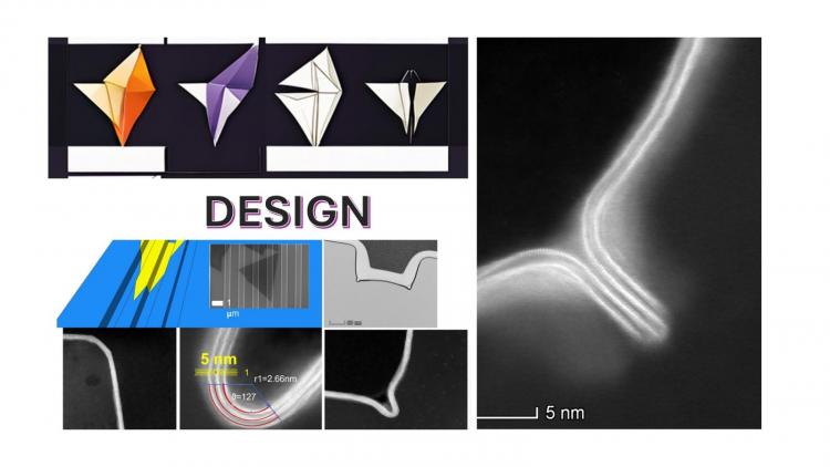
The DESIGN project, involving research units with solid expertise in material growth and characterization, nano fabrication, and theoretical modelling, aims at developing strategies, beyond the state-of-the-art, for shape engineering in 2D materials directly in the early stage of their growth. The first objective of the DESIGN project is to establish a synergistic combination between chemical vapour deposition (CVD) and thermal-Scanning Probe nano Lithography (t-SPL) to obtain shape-engineered 2D TMDs (MoS2 and WS2) by means of conformal growth of high-quality single crystals, down to the monolayer limit, onto nanopatterned templates. The second objective is to develop a framework in which to provide experimental characterization and theoretical understanding of the underlying mechanisms at stake in 2D material shape-engineering. The final objective of the DESIGN project concerns the development of “proof of concept” devices, based on the engineered 2D materials, to provide evidence of their technological interest in terms of opto-electronic properties tailored by design, which will include electron mobility boosting and photoluminescence emission tuning.
CNR Principal Investigator: Christian Martella


