
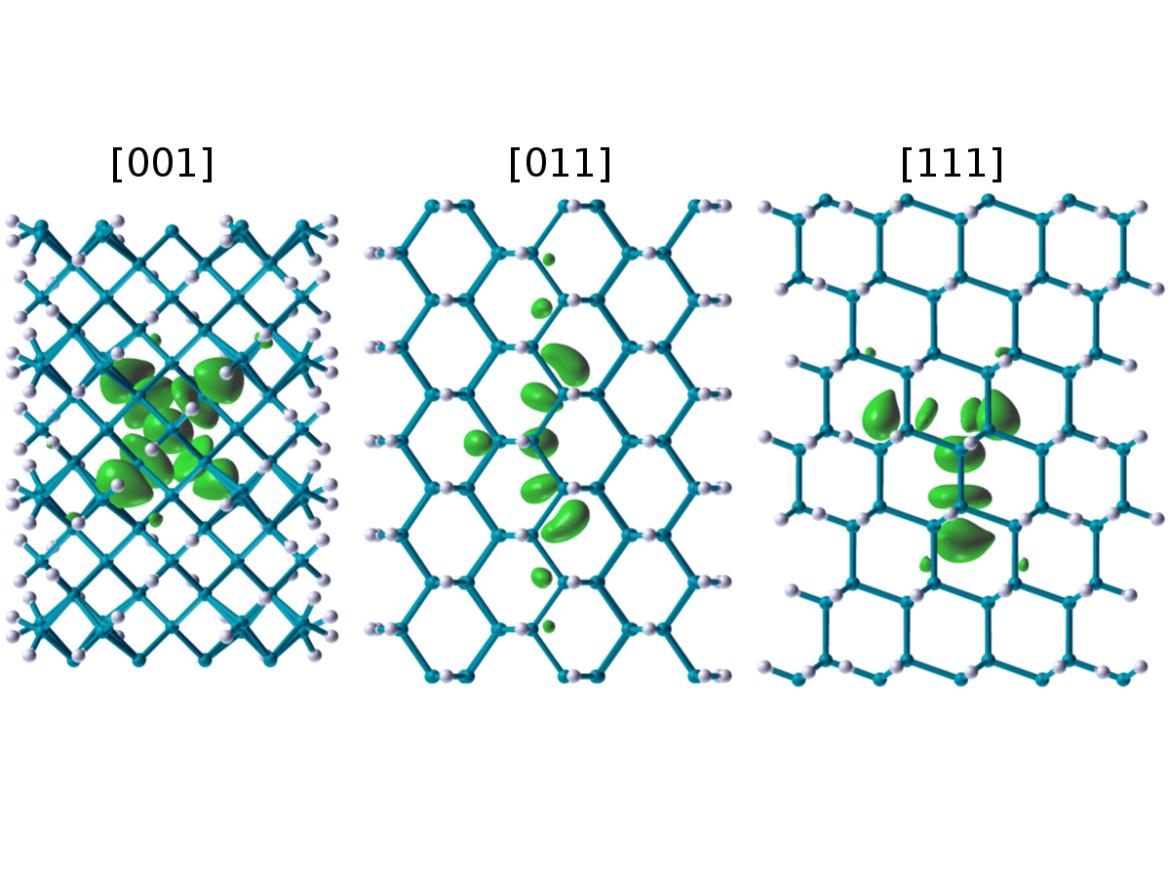
The doping of semiconductors is a key element for the production of semiconductor devices, and it has been widely studied for bulk crystals. The possibility of realizing semiconductor nanowires with dimensions down to few nanometers has stimulated a great deal of theoretical and experimental research to obtain efficient doping in view of applications in photovoltaics, photonics, electronic devices, and quantum information. By fully ab initio calculations we studied the effect of donor impurities in H passivated Silicon and Germanium nanowires oriented along different crystallographic directions. Confinement in quasi-one-dimensional nanowires noticeably influence the localization of the donor electron wave function can be of key importance in various silicon applications, since it determines the interactions between neighboring donors. We showed that the delocalization of the donor electron wave function along the axis of a nanowire is much greater in [011] oriented nanowires for phosphorus and selenium donors. We also demonstrated that its value can be controlled by applying a compressive or tensile uniaxial strain. These information are essential to determine the impurity concentration of insulator-conduction transition in doped Si nanowires, which are a crucial information for the building of nanoelectronic devices based on these materials. The confinement effect has relevant consequences on the hyperfine structure of the defect, that can be exploited for advanced electronic applications in single atom electronics or quantum computing. We computed the hyperfine structure of S and Se substitutional defects in silicon and germanium nanowires. We showed that, if the tetrahedral symmetry is preserved, the hyperfine contact term is only marginally dependent on the nanowire orientation, while it can undergo drastic changes if the symmetry is lost. Further, as proved for Se doped Si nanowires [001] oriented, the hyperfine interactions increase at small diameters, as long as the nanowire is large enough to prevent surface distortion which modifies the symmetry of the donor wave function. Moreover, surface effects lead to strong differences in the hyperfine parameters depending on the Se location inside the nanowire, allowing the identification of an impurity site on the basis of electron paramagnetic resonance spectra.
Recently, by plane-wave pseudopotentials techniques we simulated silicon hyperdoped with chalcogen impurities, for opto-electronic applications.
(Contact person: Alberto Debernardi)