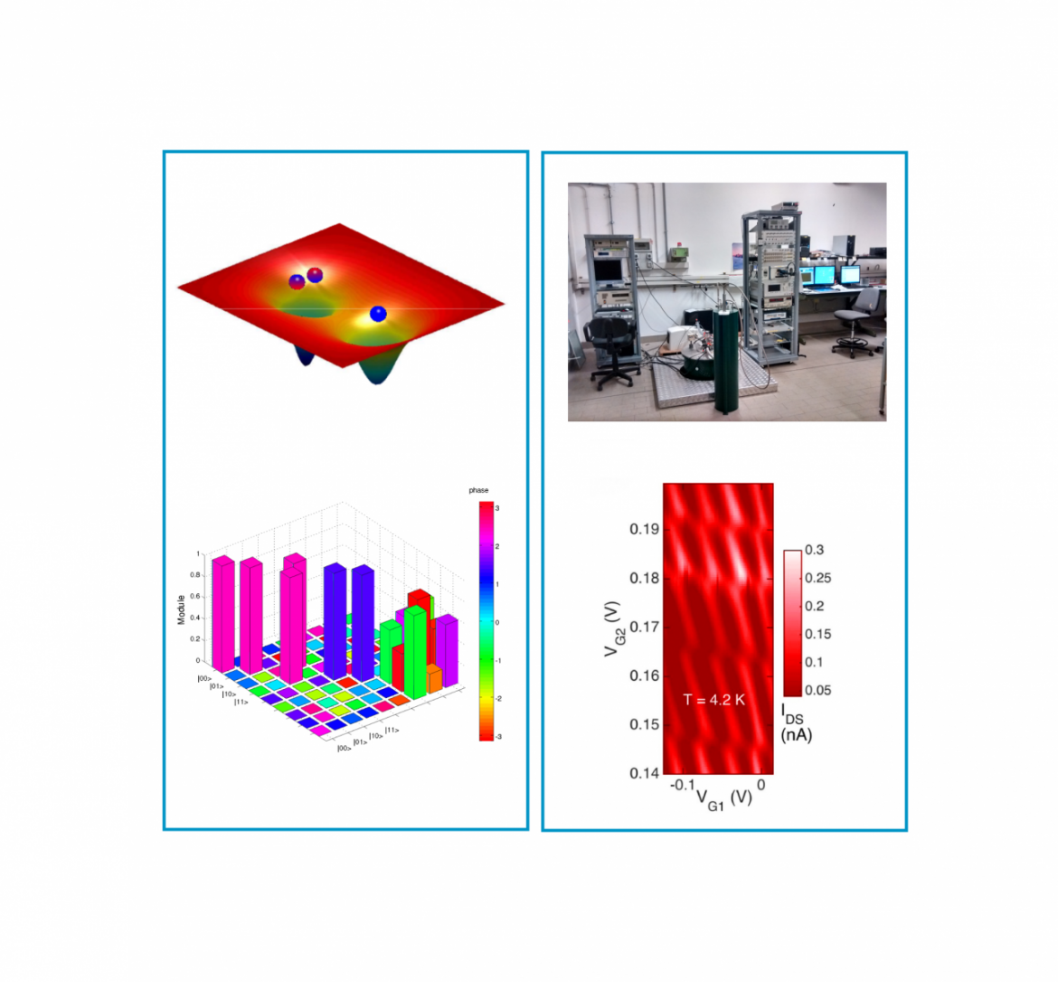
CMOS technology exploitation is crucial to fabricate in a reliable manner nanodevices where different qubits based on spin degree of freedom can be implemented. One on the goals of this activity is the identification of the most suitable physical qubit architecture in terms of scalability to pave the way to the development of solid-state quantum circuits.
In particular, the study of the modeling methodologies as future components of TCAD packages for quantum circuit design is one of the foremost subjects of the activity. Simulators based on finite element method and exploiting DFT-like approaches are used and developed for the optimization of sizes and working points of the device where the qubit is held. In order to interconnect a larger number of qubits, from a theoretical point of view the modelization of the transport mechanism through adiabatic quantum channel is investigated. Moreover, noise and decoherence effects due to the surrounding environment are evaluated and taken into account in the effective Hamiltonian models. Dynamical decoupling as well as quantum error correction schemes are studied.
From the experimental point of view, the characterization of qubit architectures (based on quantum dot spin-charge states) is expected by exploiting a constantly developed probe to interconnect the electronic set-up to the sample kept at cryogenic temperatures.
The potential applications are the realization of a quantum circuits in CMOS technology as fundamental parts of a future quantum computer, making possible the execution of calculations of non-polynomial complexity otherwise untreatable with classical computers. This will open a new way to exploit CMOS technology, limiting the detrimental effects of the Moore’s law stall and resulting in an increase of computing power to be exploited in particular fields such as imaging, cryptanalysis and large database access.
Funded project: H2020 EU project No. 688539 “MOS-QUITO” (01/04/2016 – 31/03/2019), visit http://www.mos-quito.eu for more informations.


